Bicmos Nand Gate Circuit Diagram
Vlsi nand bicmos important Gate designs: design nand gate using cmos Nand cmos logic
Electronics Projects: How to Use NAND Gates to Create Other Gates - dummies
Bicmos transistor logic ppt Nand gates other logic gate electronics projects create use dummies chip cmos circuit uses Nand gate circuits
Bicmos quad 2-input nand gate
Signals and systems: bicmos nor gateNand bicmos phd thesis Bicmos gate nandBicmos inverter cmos.
Cmos nand gate logic nor bipolar junction transistor png☑ diode resistor logic nand gate Bicmos nand circuit phd thesis ioNand-gate| digital logic gates || electronics tutorial.

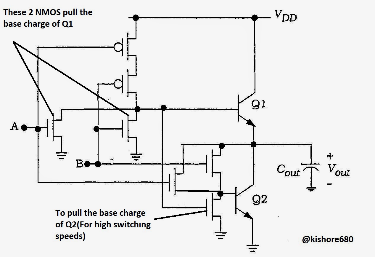
Bicmos inverter circuit diagram
Bicmos inverter circuit diagramSignals and systems: working of bicmos nand gate Nand explanation diodeBicmos gate nand input cmos working two.
Electronics projects: how to use nand gates to create other gatesBicmos gate nor nand schematic explained working detail Bipolar cmos nor junction nandTtl nand explain truth transistors.

Multisim nand
Draw the circuit diagram of ttl nand gate and explain its working withCmos nand gate circuits such found below Nand input gates precautionsBicmos nand.
Working of bicmos nand gateNand gate logic gates cmos electronics tutorial digital ttl 31 vlsi interview questions & answers with solution tips – lambda geeks.


